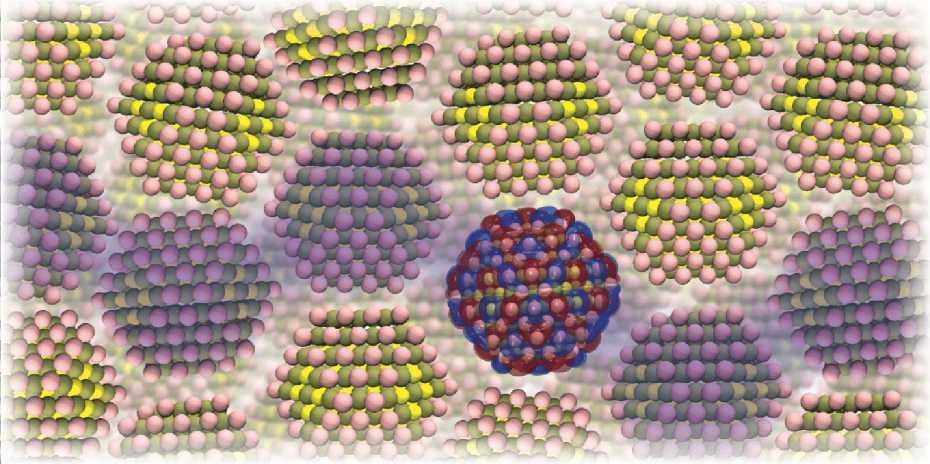
After years of research work, the way in which electric currents are conducted in nanocrystal semiconductors can now be described in detail for the first time. To achieve this, a team headed up by Professor Vanessa Wood from the Department of Information Technology and Electrical Engineering (D-ITET) at the Swiss Federal Institute of Technology in Zurich (ETH) had to mathematically describe every one of the several hundred thousand atoms in the many nanocrystals contained in semiconductor films. In addition, a description of how each atom interacts with the charge carriers was also required.
After all, in contrast to conventional semiconductors, the atoms in the crystal lattice of the nanocrystal semiconductors cannot simply be considered to be stationary points, a press release issued by ETH explains. Nuri Yazdani, a PhD student in Professor Wood’s working group and lead author of the recently published study, used the Swiss Supercomputing Centre (CSCS) at ETH in Lugano to run a complex computer program. This took into account all the details pertaining to the problem, for example the motion of the electrons and atoms as well as the interactions between them.
The results of the computer simulation showed that the tiniest deformations of the crystals, measuring just a few thousandths of a nanometer, produced a huge change in the electrostatic energy. The model explained how the electronic properties of the nanocrystal semiconductors change when the size of the nanocrystals and the way in which they are packed into the film are varied. This computer simulation perfectly predicted the electrical properties in each of the several hundred tests carried out.
“After eight years of intense work, we have now created a model that can finally quantitatively explain not just our experiments, but also those of many other research groups over the past years”, says Wood, before adding that: “Such a model will enable researchers and engineers in the future to calculate the properties of a nanocrystal semiconductor even before it is produced”.
In comparison with traditional semiconductors, nanocrystal semiconductors boast a much broader variety of electrical properties. Useful semiconductors for various applications in sensors, lasers or LEDs, in addition to TV screens, could therefore be developed in future as well.
Related news
Contact us
Can we put you in touch with a peer company or research institute? Do you need any information regarding your strategic expansion to Switzerland's technology and business center?
info@greaterzuricharea.com