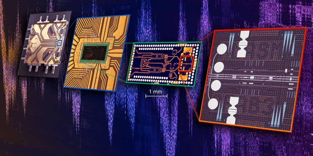
Plasmonic chip – this is the phrase on the lips of all working in the field of ultra-fast data transmission. Researchers at the Swiss Federal Institute of Technology in Zurich (ETH) have created a chip in a laboratory that directly converts electronic signals into light signals on a two-layer chip, as are used in modern transmission technologies such as fiber-optic networks. Up until now, two separate chips connected by wires were needed for this conversion. This was both expensive and slowed down data flows.
Ueli Koch, a post doctorate student in the research group headed up by Jürg Leuthold, ETH Professor of Photonics and Communications, a lead author of the study, which was published in the journal Nature Electronics, explains: “If you convert the electronic signals into light signals using separate chips, you lose a significant amount of signal quality. This also limits the speed of data transmission using light”. According to the press release issued by ETH, researchers have been trying for 20 years to combine these chips, although these attempts had always failed due to the technical need for the chips to be different sizes.
The ETH researchers have now been able to develop this new, highly compact chip in conjunction with partners based in Germany, the USA, Israel and Greece. The chip brings together the most rapid electronic and light-based construction elements in a single component for the first time, all the while ensuring practically no loss in signal quality.
“The rising demand will call for new solutions”, comments Leuthold. “The key to this paradigm shift lies in combining electronic and photonic elements on a single chip”.
For this combination, the researchers turned to plasmonics and not, as was previously the case, to photonics. “We’ve now overcome the size difference between photonics and electronics by replacing the photonics with plasmonics”, Leuthold explains. With plasmonics, light waves can be squeezed into structures that are much smaller than the wavelength of the light. Due to the fact that plasmonic chips are smaller than electronic ones, it is now possible to produce more compact, monolithic chips that feature both a photonic and an electronic layer.
Related news
Contact us
Can we put you in touch with a peer company or research institute? Do you need any information regarding your strategic expansion to Switzerland's technology and business center?
info@greaterzuricharea.com